Friday, January 14, 2011

Gold Sculptures

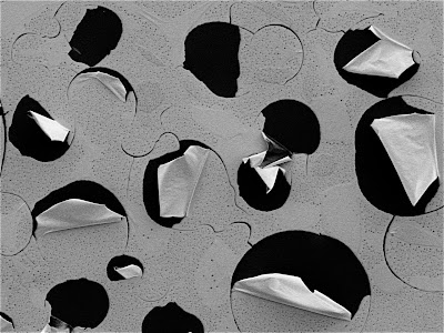
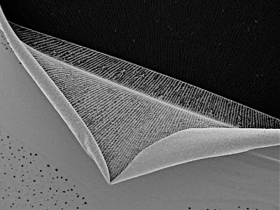
These thin films of gold (Au) were patterned into rectangles and engineered to roll up into tubes due to thermal stress built in to the films during deposition. In the following cases they failed to roll into tubes as desired, but instead rolled into other various nano-sculptures.


Wednesday, January 12, 2011

Beautiful Failures - Optical Microscope Images of Cracked GaAs Thin Films

This is an assembled collection of optical microscope images of a roughly 100 nm thin film of the semiconductor material GaAs. The thin layer was transferred from one substrate to another and in the process endured stresses which caused the film to crack. The cracking patterns are manifestations of the crystal structure of the material, which causes it to break up mostly in right angels.


Sunday, January 9, 2011

Electromagnetic Art 2

Here are some electromagnetic art images which I was fortunate to come across via people whom I work with at Caltech. The first is a collage of still images from a video showing the time evolution of the electromagnetic field as a dipole source is injected into the gap of a nanoplasmonic split dipole antenna. The simulation was run and the image was compiled by a post-doc in my group Deirdre O'Carroll, I edited it a little bit and changed the colors...


This next image I came across while going through simulation results that another post-doc in my group, Jonathan Grandidier performed of a silicon dioxide (glass) sphere which resonantly couples free space sunlight into an underlying solar cell...


Saturday, January 8, 2011

Electromagnetic Art 1

These images were created with data from finite difference time domain (FDTD) simulations which calculate the time evolution of the electromagnetic field through a specified geometry. The first is of various surface plasmon modes of a square metal-insulator-metal structure. Each square represents a different wavelength, and hence a different modal profile.


This second image is similar to the first except that the geometry which the light is propagating through is an assembly of dielectric spheres rather than metal squares as above...


Thursday, January 6, 2011

TEM Abstractions

These images were originally TEM micrographs which I then edited with various software such as ImageJ, Photoshop, etc. They bare little resemblance to the original images, but definitely would not have been created without them.


Wednesday, January 5, 2011

Transmission Electron Microscope (TEM) Images of Molybdenum Trioxide Crystals

These are 2 TEM images of crystals of molybdenum trioxide (MoO3) and impurities (black spheres) on a holey carbon grid (large holes in background). They were taken in the Materials Science Department at the California Institute of Technology on a Phillips EM420 TEM at 120keV accelerating voltage and at 37,000x magnification. The images were also edited with the scientific image analysis software, ImageJ, to produce the connected white lines within the features.


Monday, January 3, 2011

Scanning Electron Microscope (SEM) Images of Gold Thin Film


These scanning electron microscope (SEM) images are of thin films of gold (Au) deposited by thermal evaporation onto the soft polymer polymethylmethacrylate (PMMA), also known as Plexiglass. The thickness of the deposited Au films were less than 100 nm. The Au films peeled up in various places when heated due to stress related to differences in thermal expansion of the two materials.


This last image was artificially colored with Adobe Photoshop.